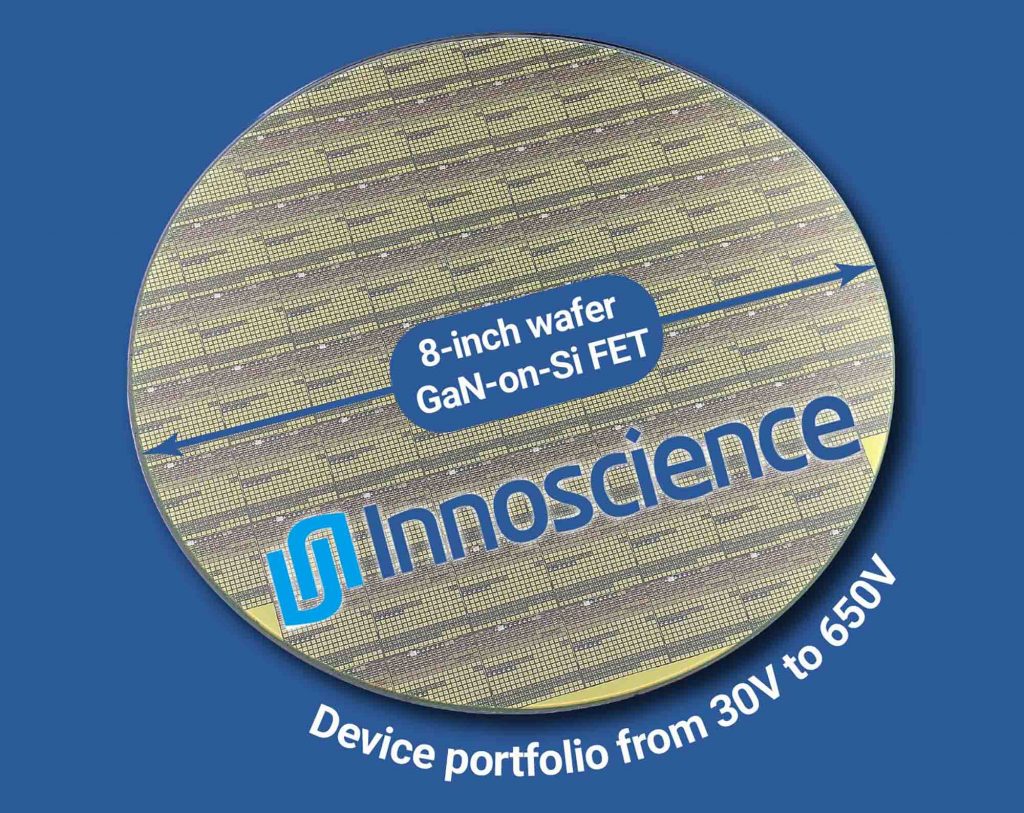
Innoscience is the world’s largest Integrated Device Manufacturer (IDM) that is fully focused on GaN technology. Innoscience’s vision is to create an energy ecosystem with effective and low-cost Gallium-Nitride-on-Silicon (GaN-on-Si) power solutions. Founded in December 2015 with investment from CMBI, ARM, SK and other prestigious investors, Innoscience has two wafer fabs including the world’s largest dedicated 8-inch GaN-on-Si site.
Currently the company has a capacity of over 14,000 8-inch wafers per month which will ramp up to 70,000 8-inch wafers per month by 2025. The company has a wide portfolio of 30 – 150V and 650V e-mode GaN-on-Si transistors. Innoscience’s GaN technology has reached consistently high international standards including advanced qualifications and reliability testing.
The company has 1,400+ employees with over 300 R&D experts that are dedicated to delivering high performance and high reliability GaN power devices that can be widely used in diverse applications including cloud computing, electric vehicles (EV) and automotive, portable devices, mobile phones, chargers and adapters.
Easy Engineering: What are the main areas of activity of the company?
INNOSCIENCE: GaN HEMTs and ICs
E.E: What’s the news about new products?
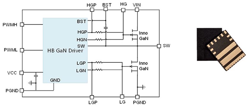
INNOSCIENCE: The first in a new family of SolidGaN integrated GaN devices, ISG3201 is a complete half-bridge circuit including two 100V 3.2mΩ InnoGaN HEMTs and the required driver circuitry in an LGA package measuring just 5×6.5×1.1mm.

The ISG3201 SolidGaN half-bridge comprises two 100V 3.2mΩ e-mode GaN HEMTs with driver, driving resistor, bootstrap and Vcc capacitors. It has a 34A continuous current capability, zero reverse recovery charge and ultra-low on resistance. Thanks to the high level of integration, gate loop and power loop parasitics are kept below 1nH. As a result, voltage spikes on switching nodes are minimized. The Turn-On speed of the half-bridge GaN HEMTs can be adjusted using a single resistor.
ISG3201 is suitable for high frequency Buck converters, half-bridge or full-bridge converters, Class D audio amplifiers, LLC converters and power modules. Overall, the integrated ISG3201 solution can save up to 20% PCB space on discrete GaN designs and 73% board space on traditional silicon implementations.
Bi-GaN bi-directional GaN HEMTs save space and facilitate fast charging without suffering from reliability-limiting and potentially dangerous rises in temperature that can sometimes be seen in traditional silicon devices. Innoscience has also revealed that leading consumer electronics and mobile communications company, OPPO, is using the new BiGaN devices inside its phone handset to control the battery’s charging and discharging currents. This is the first time that such protection, based on GaN technology, has been included in the phone itself – previously the circuitry had to be incorporated inside the charger.
Thanks to InnoGaN’s low RDS(on), the fact that it does not have parasitic diodes, and the unique bidirectional feature of Innoscience’s BiGaN technology, one BiGaN HEMT can be used to replace back-to-back connected NMOS MOSFETs in a common-source configuration to achieve bi-directional switching of the battery’s charging and discharging currents. This reduces on-state resistance by 50%, chip size by 70%, and temperature rise by 40%.
The first BiGaN device generally released by Innoscience is the INN040W0488, a 40V bi-directional GaN-on-silicon HEMT in the WLCSP package measuring 2.1mm x 2.1mm.
INN40W08 40V bi-directional GaN-on-Si enhancement mode high-electron-mobility-transistors (HEMT) target mobile devices, including laptops and cellular phones. The INN40W08 HEMT has been developed using the company’s advanced InnoGaN technology which features ultra-low on resistance.
Featuring a bi-directional blocking capability, the new INN40W08 GaN HEMTs have a ultra-low on resistance of just 7.8 mΩ. This is achieved by the company’s advanced InnoGaN patented strain enhancement layer technology which reduces sheet resistance by 66%. Gate charge (QG) is typically 12.7nC. The 5×5 grid wafer level chip scale package (WLCSP) measures just 2×2 mm. This small footprint enables INN40W08 GaN HEMTs to be integrated inside mobile phones.
E.E: What are the ranges of products?
- 30 – 150V and 650V e-mode GaN-on-Si transistors.
- SolidGaN integrated GaN devices such as the ISG3201, a complete half-bridge circuit
- Bi-GaN bi-directional GaN HEMTs
E.E: At what stage is the market where you are currently active?
INNOSCIENCE: The market for GaN power devices is exploding, because GaN enables high efficiency switching, which reduces heat, eliminating fans and heatsinks, shrinking device size and saving BOM cost.

E.E: What can you tell us about market trends?
INNOSCIENCE: The key drivers for the switch to GaN is the need to produce smaller, more efficient and possibly cheaper power converters. The main challenge has been the same as the move to any new technology: building confidence. But today mostly that has been addressed: Innoscience HEMTs have been used in USB-PD laptop chargers that are one third the size of silicon-based devices; ebike chargers made in GaN have been reduced in dimensions by 75% so that they fit in a backpack; and DC/DC converters for data centres made with Innoscience’s InnoGaN is half the size of silicon, and also much more efficient, reducing energy consumption. The performance advantages of GaN are well understood, and the challenges of driving GaN HEMTs have been overcome, and evidence from companies such as Innoscience point to reliability figures which are on a par with silicon.
We see a trend of companies talking about 8-inch wafer fabrication: Innoscience is already there.
E.E: What estimations do you have for 2023?
INNOSCIENCE: Silicon is still currently cheaper at the device level. But as GaN moves to 8-inch mass-production with economies of scale, then that gap will decrease. Thanks to Innoscience’s investment in 8-inch wafer fabs, the price-gap has already shrunk to a small percentage (and not a multiple as some years ago). As you move up to the module level and system level, then GaN is already cheaper, so any difference in price between silicon and GaN is paid back at the BOM cost.
As a manufacturer we are also in a position to investigate new materials, and I am excited about new epitaxies that will reduce the cost of material.
We are also looking to reduce the specific ON resistance and widen the maximum gate voltage range.

