

Powered by its in-house SPIN software platform, Stratus Vision delivers specialized inspection solutions, including the INREMA photomask system, wire-bond verification down to 10 µm gold wires, and Through Glass Via (TGV) inspection for 2.5D and 3D chiplet integration. Driven by European supply chain sovereignty under the EU Chips Act 2.0 and expanding pilot lines in Taiwan, the company is bridging the gap left by aging legacy systems while establishing new benchmarks for AI-driven defect classification.
Ronald Stenger, Managing Director of Stratus Vision GmbH, outlines the expansion of the Bavarian company’s automated optical inspection (AOI) technology across the global semiconductor supply chain.
A brief description of the company and its activities.
Ronald Stenger: Stratus Vision GmbH is an owner-managed Bavarian family business headquartered in Puchheim near Munich. Founded in 2003, we develop and manufacture automated optical inspection systems for the semiconductor industry and adjacent high-precision markets. Over more than two decades of continuous development, we have delivered more than 120 inspection systems to customers worldwide. All our products run on our proprietary software platform SPIN, developed and refined in-house. Hardware and software are entirely developed and produced in Bavaria, by a lean team focused on high-precision optical inspection.
What are the main areas of activity of the company?
R.S: Our activities cluster around four main pillars: photomask inspection for the semiconductor front-end, wire-bond inspection for power module manufacturing in automotive and power electronics, Through Glass Via (TGV) inspection for advanced packaging, and special-purpose optical inspection for ceramics, medical technology, defense and industrial applications. All four pillars share our SPIN software platform, which allows us to leverage more than two decades of accumulated inspection know-how across very different physical inspection tasks.
What’s the news about new products/services?
R.S: We are actively developing three concrete new capabilities. First, the INREMA platform is being redesigned with an integrated Filter Fan Unit and an optional Equipment Front End Module (EFEM), making it fully integrable into modern automated mask-shop lines. Our first reference customer for this configuration is already secured. Second, we are launching Bright Light Visual Check (BLV), a fully automated inspection of the pellicle assembly from all sides after its application onto the photomask. This inspection step has never been consistently automated worldwide. The feasibility study has been completed successfully; the first installation is scheduled for 2027 in an ISO Class 1 cleanroom environment. Third, we are extending our wire-bond inspection capability down to 10 µm gold wires with full height mapping, addressing the finest-pitch bonding requirements in modern power modules and high-frequency devices.
What are the ranges of products/services?
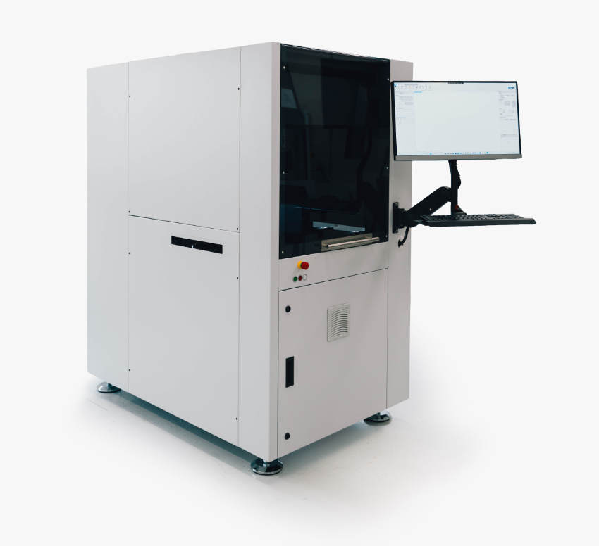
R.S: Our current product range covers four established lines. INREMA is our CAD-based photomask inspection system, covering the full format range from 5 to 14 inch, with defect detection down to 100 nm and die-to-database setup in under five minutes. Our wire-bond inspection systems provide optical quality assurance of bond wires in power module manufacturing, with a proprietary AI-driven defect classification. Our TGV inspection system addresses Through Glass Via inspection for 2.5D and 3D chiplet integration in advanced packaging. Alongside these, we offer custom-engineered inspection solutions for special applications in ceramics, medical technology, defense and industrial precision markets. All systems run on SPIN, our shared software platform that ensures consistent operation and significantly reduces the learning curve for operators.
What is the state of the market where you are currently active?
R.S: The markets we serve are all in active growth phases, each driven by distinct forces. Photomask inspection is expanding on the back of sustained demand for mature-node chips used in automotive, industrial and IoT applications. The installed base at European mask shops is aging, and vendor support from the incumbent US suppliers is progressively winding down, which opens a significant replacement window over the coming years. The advanced packaging market is at a genuinely new phase: as classical transistor scaling reaches its economic limits, the industry is pivoting into chiplet integration on interposers and glass substrates, creating a wave of inspection requirements that did not exist five years ago. In power module manufacturing, the electrification of transport and industrial systems is driving double-digit annual growth, and inspection intensity is rising as SiC and GaN devices require tighter defect control than legacy silicon. Across all three, European industrial policy is shifting weight toward supply chain sovereignty, backed by the EU Chips Act 2.0 designation of photomask inspection equipment as a Critical Supply Chain Facility category.
What can you tell us about market trends?
R.S: Three trends are shaping our roadmap. First, advanced packaging and chiplet integration are absorbing a rapidly growing share of semiconductor value creation as classical node scaling reaches physical and economic limits. Second, supply chain sovereignty has moved from talking point to policy driver in Europe, backed by the EU Chips Act 2.0 and national programs such as the Bavarian Semiconductor Initiative. European suppliers of critical semiconductor equipment are gaining unprecedented political attention. Third, AI-driven defect classification is transitioning from differentiator to industry standard. Our SPIN platform integrates a proprietary AI engine that gives us a significant lead in throughput, accuracy and adaptability to new defect classes.
What are the most innovative products/services marketed?
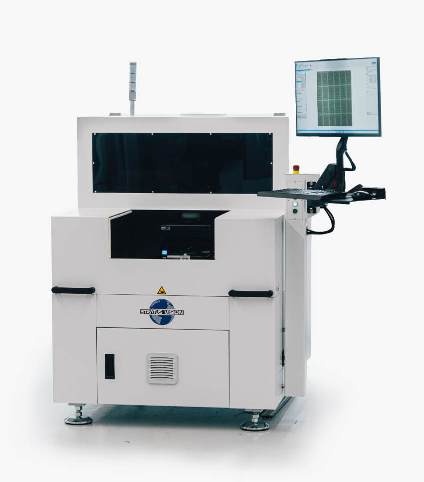
R.S: Our most innovative offering combines the INREMA platform with its new EFEM configuration and the TGV inspection system. INREMA is the only European automated optical inspection platform that covers the full photomask format range from 5 to 14 inch with a single modular hardware kit, at a fraction of the total cost of ownership of comparable systems. The upcoming EFEM-integrated version turns INREMA from a stand-alone tool into fab-line equipment, addressing the next investment cycle at European mask shops. TGV inspection addresses a genuinely new market: the inspection of glass substrates with through-glass vias for 2.5D and 3D advanced packaging. We currently have multiple TGV systems installed, and together with our customer and sales agent in Taiwan we are building up a pilot line featuring our tool in the world’s densest semiconductor ecosystem.
What estimations do you have for the second half of 2026?
R.S: The second half of 2026 will be centered on three parallel tracks. We will continue the rollout of INREMA at existing photomask customers, driven by the aging KLA and Applied Materials installed base in Europe. We will advance our platform redesign to full readiness for integration into modern automated mask-shop lines, with the first EFEM-configured system going into customer operation. And we will scale our TGV inspection presence through the Taiwan pilot line, using it as a strategic anchor for foundry and OSAT customer relationships across Asia. In parallel, we expect strong momentum in our power module inspection business, driven by the ongoing electrification wave in automotive and industrial applications, where our AI-driven defect classification is delivering a measurable production advantage.