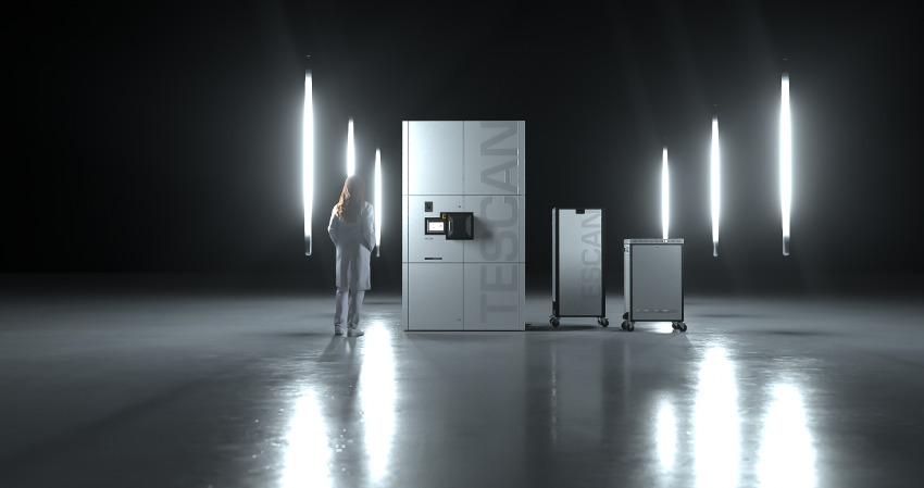
TESCAN Group is a trusted global provider of innovative technologies for science and industry, with over 30 years of experience in developing electron microscopy, micro-computed tomography, and related software solutions. With a presence in 14 branches worldwide and more than 750 employees, TESCAN Group enables scientists and engineers to solve complex challenges at the micro and nano levels. The company’s headquarters is in Brno, Czech Republic.
Interview with Petr Klímek, Product Marketing Director at TESCAN.
What are the main areas of activity of the company?
Petr Klímek: TESCAN Group enables scientists and engineers to address global and sustainability challenges with innovative instrumentation that reveals, uncovers, and discovers the secrets of matter at the micro and nano scale. TESCAN transforms highly complex technologies into simplified solutions, equipping any user to pursue their goals. TESCAN strives to be a people-oriented organization, continuously developing its employees to enhance the experience of our partners in business through professionalism, passion, and openness.
TESCAN products can be easily divided into 5 groups according to the technology used. Scanning Electron Microscopes (SEM), SEMs equipped with Ga and/or Plasma Focussed Ion Beam Systems (FIB-SEM), Analytical Scanning Transmission Electron Microscopy (STEM), Micro-CT and UHV systems.
What’s the news about new products/services?
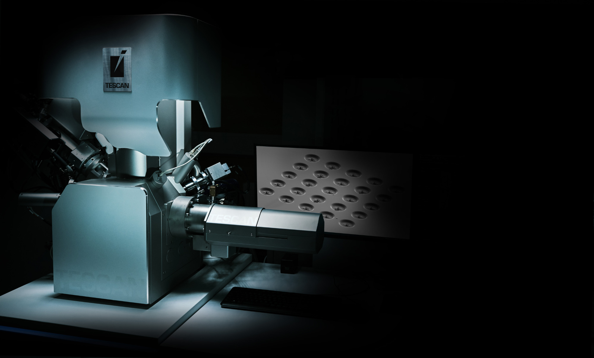
P.K: In 2024, TESCAN solidified its position as a leader in scientific innovation with the launch of two flagship products, AMBER 2 and AMBER X 2, marking a transformative moment for the company and the field of materials science. The TESCAN AMBER 2 is a fully automated Ga FIB-SEM system designed for routine TEM sample preparation, nanoscale characterization, and prototyping. Alongside this, TESCAN introduced the AURA Gentle Ion Beam system, which minimizes damage during TEM specimen preparation, and the TEM AutoPrep Pro™ software for automated sample preparation.
The TESCAN AMBER X 2, launched later in the year, redefines plasma FIB-SEM technology with unmatched resolution, throughput, and versatility, making it ideal for multi-user facilities and central laboratories.
What are the ranges of products/services?
P.K: TESCAN offers a comprehensive range of products categorized by technology, including:
- Scanning Transmission Electron Microscopes (STEM): Featuring the TESCAN TENSOR, the world’s first dedicated analytical 4D-STEM system for nanoscale material characterization.
- Focused Ion Beam Scanning Electron Microscopes (FIB-SEM): A variety of systems with both Ga and Xe plasma options, including the TESCAN AMBER 2 and AMBER X 2, designed for high-resolution imaging and sample preparation.
- Scanning Electron Microscopes (SEM): From the versatile TESCAN VEGA for routine SEM analysis, to high-resolution systems like the TESCAN MIRA, CLARA, and MAGNA.
- Micro-Computed Tomography (Micro-CT): A range of micro-CT systems for non-destructive testing, such as the TESCAN UniTOM XL, DynaTOM, and CoreTOM.
- Special Solutions: Customized systems for specialized applications, including the TESCAN TIMA for automated mineral analysis, TESCAN RISE for correlative Raman-SEM imaging, and UHV FIB-SEM with integrated glovebox for controlled environments.
TESCAN’s versatile product lineup supports diverse applications across materials science, life sciences, geosciences, and semiconductor research.
What is the state of the market where you are currently active?
P.K: The global electron microscopy market is experiencing significant growth, driven by expanding applications in semiconductors, life sciences, and materials science. The market is currently valued at approximately $3.62 billion and is expected to grow at a compound annual growth rate (CAGR) between 5-8% through 2028, depending on the market segment. While North America and Europe represent significant markets, rapid growth is anticipated in the Asia-Pacific region due to increased research investments and interest in semiconductor applications.
What can you tell us about market trends?
P.K: In the academic sector, the electron microscopy market is seeing a growing demand for highly automated, open-access, multimodal platforms that integrate seamlessly into specific research workflows. Researchers and industry professionals increasingly seek solutions that support interoperability, allowing easy data transfer and collaboration across different imaging and analytical systems. By leveraging AI algorithms, gaining the maximum number of modalities (data points) from a sample area has become significantly easier.

Moreover, the successful integration of AI-driven automation into electron microscopy workflows has enabled more efficient quality control and failure analysis, particularly in the semiconductor field. These AI-enhanced systems help to reduce manual workload and improve throughput.
What are the most innovative products/services marketed?
P.K: From TESCAN’s perspective, the AMBER X 2 and TESCAN TENSOR have emerged as groundbreaking products. The AMBER X uniquely combines attributes typically associated with Gallium (Ga) FIB, with the speed and versatility of Plasma FIB. This allows users to switch seamlessly between high-precision and large-scale applications on a single platform, enabling a broad range of tasks with unmatched speed and efficiency.
Complementing this, the TESCAN TENSOR offers an ultimate STEM platform tailored for nanoscale STEM, 4D STEM, and Electron Dispersive Spectroscopy (EDS) analysis. The TENSOR is engineered for analytical studies of materials at the nanoscale, providing unmatched detail in both compositional and structural analyses. This makes it a premier choice for researchers needing high-resolution analytical insights into complex materials. Together, the AMBER X and TESCAN TENSOR exemplify how innovation in electron microscopy can elevate both the precision and versatility of material characterization and analysis.
What estimations do you have for the rest of 2024?
P.K: For the rest of 2024, we anticipate strong growth and traction, particularly with our high-end products. The AMBER X 2, newly released, has received extremely positive feedback, with industry professionals consistently acknowledging it as a transformative innovation in the FIB-SEM landscape. This reinforces our position in the market and opens doors to new applications that benefit from its unrestricted Plasma FIB capabilities.
Similarly, the TESCAN TENSOR has garnered significant interest globally. We are seeing high demand from prominent research institutions and industry leaders who recognize the TENSOR’s potential to deliver unparalleled STEM, EDS, and 4D STEM analyses at the nanoscale and unprecedented ease of use. We expect several high-level sites across various regions to finalize purchases, which will further solidify our footprint in the TEM/STEM market segment. With these positive developments, we are on track to end the year with substantial gains in market share and set the stage for continued success into 2025.